碳化矽磊晶片應用於多種電子零件,例如:肖特基二極管(Shockley diode)、金屬氧化物半導體場效應電晶體(MOSFET)、結型場效應電晶體(JFET)、雙極性電晶體(BJT)、晶閘管(Thyristor)、 可關斷晶閘管(GTO)和絕緣柵雙極型電晶體(IGBT)。請參閱我們4"~6"碳化矽之規格,或連繫我們。
(一) 4H碳化矽磊晶片標準規格 (150mm & 100mm & 76.2mm)
| Substrate orientation : Epitaxy is only available for off-axis substrates | ||
| Doping | ||
| n-type | p-type | |
| Dopant | Nitrogen | Aluminum |
| Net Doping Density | ND-NA | NA-ND |
| Silicon Face | 9E14~1E19cm-3 | 9E14~1E19cm-3 |
| Tolerance | ± 15% | ± 50% |
| Uniformity | ≦ 10% | ≦ 20% |
| Thickness: 0.2~100µm | ||
| Tolerance | ± 10% | |
| Uniformity | ≦ 5% | |
(二) 4H碳化矽磊晶片產品規範(150mm & 100mm & 76.2mm)
| Characteristics | Acceptable Limits | Definitions | Test Methods |
| Epi Defects | 2mm*2mm die yield ≥ 95% |
Defects only include triangular defects, downfalls, carrots and comets. | Candela CS920 |
| Edge Chips | ≦ 2 with radius 1.5mm | Areas where material has been unintentionally peeled off from the wafer | High Intensity illumination |
| Scratches | ≦ 10 lines total and the total length of these lines should be less than wafer diameter | Grooves or cuts below the surface plane of the wafer having a length-to-width ratio of greater than 5 to 1 | |
| Surface Roughness | <0.5mm | 20µm*20µm scanned by AFM | |
| Backside Cleanliness | 100% clean | None contamination | |
| Thickness | see specification table | Thickness is determined as an average value across the wafer by FTIR | FTIR |
| Net doping | see specification table | Net doping is determined as an average value across the wafer by MCV. | MCV |
(三) 碳化矽磊晶片厚度均勻性分布圖
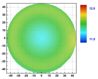
| mean value(µm): | 12.04 |
| sigma/mean: | 1.28% |
| (max-min)/(max+min): | 3.04% |
(四) 碳化矽磊晶片摻雜均勻性分布圖
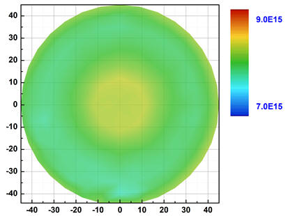
| mean value(cm-3): | 7.9515 |
| sigma/mean: | 3.48% |
| (max-min)/(max+min): | 9.97% |